The surface of next-generation lasers will be tailored in a way that allows one to replace current optics. The advantages are that the laser will be smaller and can be built as a single unit. Researchers at Chalmers University of Technology hope to develop the technology and identify new applications.
Project Grant 2020
Metasurface-emitting lasers: Tomorrow’s light sources for applied photonics
Principal investigator:
Professor Mikael Käll
Co-investigators:
Chalmers University of Technology
Åsa Haglund
Anders Larsson
Philippe Tassin
Institution:
Chalmers University of Technology
Grant in SEK:
SEK 38.1 million over five years
These days lasers are key components in many technologies. Laser light not only carries information in our fiber networks, it is also used in facial recognition and to control self-driving vehicles. Furthermore, laser light is used in new methods in the fields of bioscience and medicine.
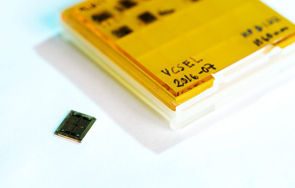
One particular kind of laser technology has driven development, the vertical-cavity surface-emitting laser (VCSEL). It takes up very little space, and can therefore be used in consumer devices such as mobile phones.
But like all laser technology, the VCSEL needs optical components to achieve the desired results. A new project funded by Knut and Alice Wallenberg Foundation aims to build the optics into the laser itself. The route the researchers are taking involves something called “metasurfaces”.
The concept of metasurfaces is well established in nanooptics. It entails coating a material with an ultrathin film of nanoparticles in a tailored structure. Although the metasurface is thinner than the wavelength of the light, it possesses properties that govern how the light is refracted or reflected. Among the more imaginative uses of metasurfaces are coatings that can make objects virtually invisible.
The metasurface can be designed to work as an optical lens, for example. When a VCSEL is coated with a metasurface of this kind, an external lens is no longer needed. The result is a single device that can be manufactured in one process.
“This enables us to build ultra-compact devices containing electronics, light source and optics. These units may ultimately be both cheaper and simpler to make than current lasers, and lead to more energy-efficient devices,” says Mikael Käll, professor at Chalmers University of Technology.
World-leading research
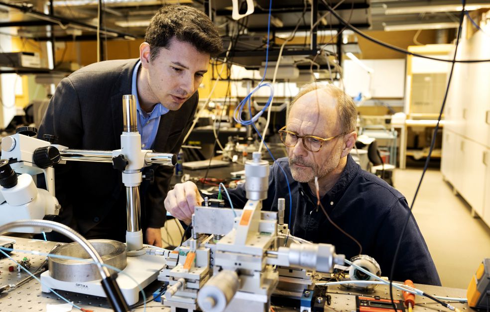
The project brings together multiple research teams from Chalmers, where knowledge of lasers, and VCSEL in particular, is world-leading. Åsa Haglund’s team is developing VCSELs for blue and ultraviolet light, while Anders Larsson’s group is concentrating on lasers that produce near-infrared light. Additional knowledge is being provided by theoretician Philippe Tassin.
The researchers are carrying out the project in parallel stages, among the first of which is to create a unit in which a metalens is etched into a laser to control the direction and focus of the light.
“We’re starting with the near-infrared since the VCSELs for these wavelengths are well established. But it’s far from simple to create the right effect in the material. We have to make extensive theoretical calculations and also find an etching process that yields the right results,” Käll explains.
The second part of the project has a more challenging goal: to etch metasurfaces within the part of the laser where the light itself is created. The metasurface can then reflect a portion of the light back into the laser, potentially simplifying control of wavelength and polarization. Here, the emphasis is on VCSELs for ultraviolet light, with Åsa Haglund’s team achieving some of the shortest wavelengths in the world.
“An even more ambitious goal is to have multiple interconnected lasers interacting with each other with the help of a metasurface. This would open the way for much more powerful lasers, and even though it’s a long shot, there are some indications that it may work,” Käll says.
New potential for microscopy
Thanks to technological developments, the project will also yield examples of new applications for lasers using metasurfaces.
“If we can succeed in making the devices as compact as we hope, we’ll be able to use the technology as new light sources in for example fluorescence microscopy, which is much used in biophysics and cell biology. Hopefully, on the strength of my earlier research, we wiIl also be able to build molecular sensors in which the laser is an integral part,” Käll explains.
Lasers with metasurfaces may also be used in the future to create miniaturized laboratories – “lab-on-a-chip”. They may also improve the technology used for facial recognition, and determining distance in self-driving vehicles.
Major challenges
The numerous challenges facing the researchers include the theoretical calculations needed to understand how the light integrates with the metasurfaces, and the difficult nanoscale etching processes that will be required. In the design phase they will be using various AI methods, such as deep learning.
“Even if we do everything right, there are no guarantees it will be as effective as we hope. If the units we create are to have practical applications, they will have to be better than their current counterparts. This is a dynamic research field in which many international research teams are active, but we believe we possess the expertise to make an impression.”
The project has given the researchers from Chalmers a long-awaited chance to collaborate:
“We have had numerous discussions over the years without finding a way to work together. The grant we have received from Knut and Alice Wallenberg Foundation has given us a common goal. We hope to make a difference in this field,” Käll adds.
Text Magnus Trogen Pahlén
Translation Maxwell Arding
Photo Johan Wingborg
Wallenberg Scholars
Driving particles with the power of light
Project Grant 2012
Optical antennas that make the nanoworld visible