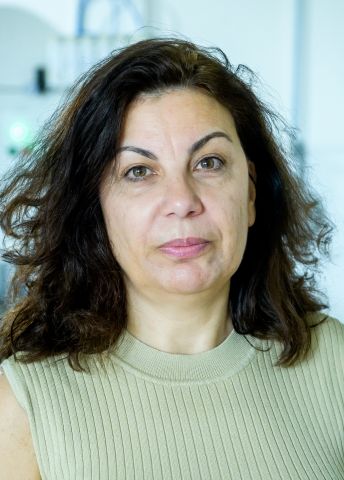
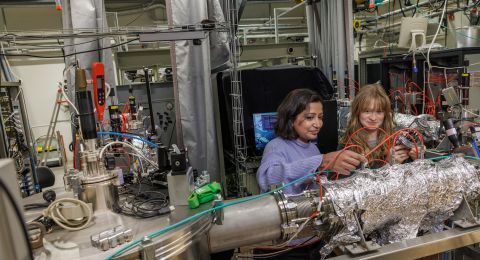
Semiconductor chips that are smaller, more efficient and cheaper are the goal of Vanya Darakchieva’s research. She wants to develop semiconductors with a wider bandgap, thereby enhancing the performance of the material.
Vanya Darakchieva
Professor of Solid-State Physics
Wallenberg Scholar
Institution:
Lund University
Research field:
Semiconductor materials, energy efficiency and performance
“A wider bandgap enables the material to cope with higher temperatures, voltage and current. This will in turn enable us to make much more energy-efficient components with higher capacity,” says Darakchieva, who is a professor of solid-state physics and a Wallenberg Scholar at Lund University.
In semiconductor components the ability to conduct electricity can be controlled. This is a key element in all modern electronics. In semiconducting materials, the energy levels of the electrons form energy bands, separated by a bandgap. Under some circumstances electrons can get enough energy to jump the bandgap, causing the material to become conductive.
Current semiconductor chips are largely based on silicon compounds with small bandgaps. They have been easiest to use, but over time materials with wider bandgaps have been developed for use in LEDs and for other purposes. Darakchieva wants to move on to “ultrawide” bandgaps.
“There has been relatively little development work in this field so far. After all, there’s no shortage of naturally occurring silicon and there has until recently been no pressure to go beyond ‘state-of-the-art.’ People seldom do, unfortunately.”
But demands are changing. Darakchieva highlights society’s need for more energy, efficient use of electricity, faster communications, larger data quantities, more energy-efficient base stations for 6G networks… Ultrawide bandgaps could be part of the solution.
Harder to maintain control as bandgaps grow
The new materials will be metal oxides or nitrides. Gallium nitride is already being used for LEDs because of its wide bandgaps. Darakchieva is examining the properties of gallium nitride and aluminum nitride to see whether either or both of them in combination might work. But as bandgaps grow, some properties become harder to control. When semiconductors are created, defects are deliberately incorporated in the crystal structure of the material by removing atoms or replacing them with atoms of another element. This is known as doping, a method that enables conductivity to be controlled.
“But fabricated materials are never perfect – they always have natural defects. These become harder to control as the bandgap increases,” Darakchieva explains.
The new semiconductors also need to be made of materials that are not too rare, and that cannot only be extracted in politically unstable regions. Geopolitics is an important factor for materials developers who want to see their discoveries put to use.
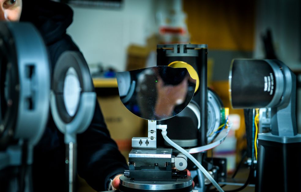
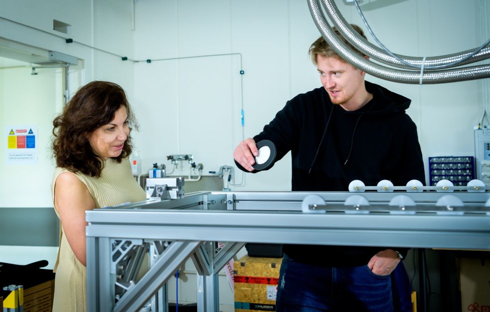
The Wallenberg Scholar grant enables Darakchieva to expand the advanced battery of instruments that her research team is using, instruments that have allowed completely new discoveries. One method involves a type of spectroscopy called ellipsometry. The technology has enabled the team to detect properties in the defects present in the semiconductor materials, properties that were previously unknown, or even misunderstood.
“We can study materials at a higher resolution than anyone has previously achieved, and discover a whole jungle of unknown physical phenomena. It’s just fantastic. In one of our labs we are studying the materials; in another we are fabricating them to see exactly what works or what is missing. It’s extremely challenging, and would normally take tens of years – but that is time we do not have. Climate change is under way and we have to find solutions quickly.”
A desire to benefit humankind
Even as a child, growing up in Bulgaria, Darakchieva knew she wanted to be a researcher. When she was ten her horrified parents found her trying to perform an experiment known as “the volcano” on the family’s veranda, attempting to ignite magnesium powder – right next to a gas cylinder used to heat water in the house.
“My punishment was that for some time, I was not allowed to pay visits to a laboratory for young researchers that I really liked…”
She soon became interested in astronomy, a field in which she retains a keen interest. She chose materials science as a way to make a contribution. Materials with ultrawide bandgaps would also be a great asset in space.
Darakchieva first came to Sweden to take up a PhD position at Linköping University. She joined a lab headed by Professor Bo Monemar, who had good contacts among some of the most pre-eminent researchers in the semiconductor field. She moved on to the U.S. and elsewhere, but when it was time for children, she wanted to return to Sweden.
“I think it’s a wonderful place, particularly for women. Sweden is a world leader in equality, good conditions and tolerance, combined with high-quality research. It’s unique.”
Ultrawide bandgaps can solve problems in electronics, and also make it possible to create new materials for quantum technology.
Her goal over the next few years is for her team to succeed in gaining complete control over the defects and doping in the new semiconductors. No one has yet managed to do this in materials with ultrawide bandgaps.
“Performing a unique and fantastic experiment is a wonderful thing for a researcher. But it’s even better if you can achieve results that benefit society – making things better for humanity. At present we are experiencing a crisis on all fronts of such magnitude that researchers must truly commit to solving it. And we are doing just that, which gives me a sense of pleasure as well as pride.”
Text Lisa Kirsebom
Translation Maxwell Arding
Photo Kennet Ruona