When researchers invented a method that allowed them to look into the world of the atom, nanoscience gained speed. The modern electron microscopes have meant that researchers can today tailor materials down to an atomic level. Xiaodong Zou will now take the electron microscope to new depths; the pictures will become three-dimensional.
Project Grants 2012
3D Electron Microscopy for Nanostructure Research
Principal investigator:
Xiaodong Zou, Professor of Structural Chemistry
Co-investigators:
Stockholm University
Lennart Bergström
Sven Hovmöller
Peter Oleynikov
German Salazar-Alvarez
Junliang Sun
Gunnar Svensson
Osamu Terasaki
Cheuk-wai Tai
Wei Wan
Polytechnic University of Valencia
Avelino Corma
University of California, Berkeley
Omar Yagh
Institution:
Stockholm University
Grant in SEK:
SEK 33.4 million over five years
“Seeing what a material looks like at an atomic level is very important to know how the material can be used. If you are not aware of the structure of the material, you are blind; you can only guess how you can make things better. The properties of a material are related to its structure,” says Xiaodong Zou, Professor of Structural Chemistry and coordinator of the new Wallenberg project ”3D Electron Microscopy for Nanostructure Research”.
She provides an example. A researcher in the project, Omar Yaghi at UC Berkeley, is developing material for gas storage in the cars of the future. The Berkeley researchers have developed an extremely porous material that means that the gas can be packed with much higher density, at the same time that the pressure in the tank becomes much lower. When the researchers now want to optimize the material, it is necessary that they see what the cavities look like and how the atoms that build the material are arranged. Only when they know this can they further improve the material so that it can store even more gas.
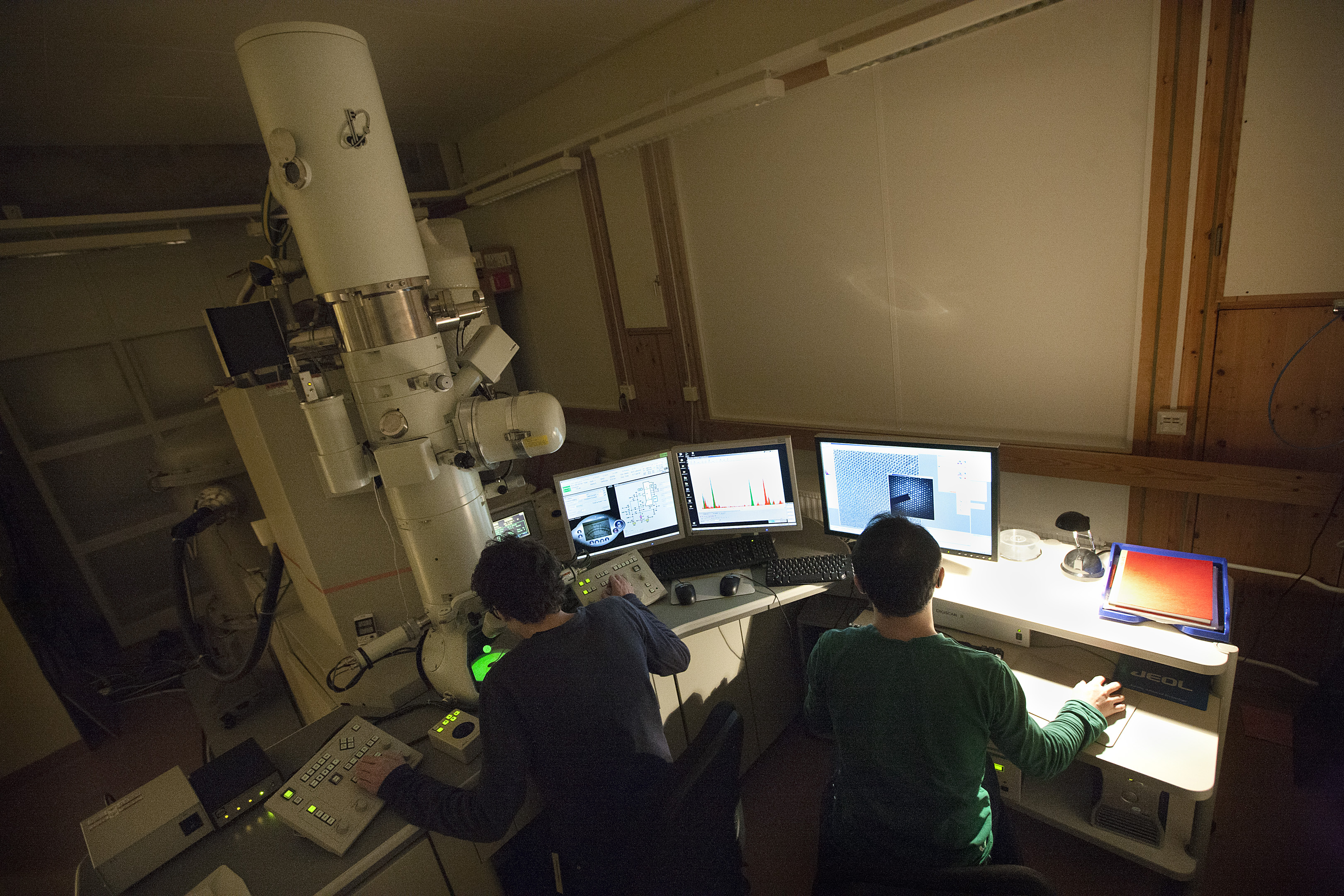
Electron beams make it possible to see individual atoms
When researchers want to investigate atoms in a material, regular light microscopes do not work because light has a long wavelength compared to the atoms. Instead of light, the researchers use electron beams with a wavelength of around 0.002-0.003 nanometers.
“The advantage of an electron microscope is that we can get pictures with a resolution at the atomic level; we can see individual atoms,” says Xiaodong Zou.
The first electron microscope was developed as early as 1931, but the resolution was much worse then. It was not until the 1970s that the technology had been improved so much that researchers could distinguish atoms of heavy metals. Today, the technology has been optimized so much that all atoms in an ordered material can be depicted.
But the pictures so far have been two dimensional. The goal of the project that Xiaodong Zou conducts is to develop a technique that makes it possible to see how the atoms are arranged in three dimensions. The researchers will be able to place a crystal of a material in a special sample holder in the electron microscope. The sample holder will then automatically rotate the crystal by less than 0.1 degrees at a time, while the microscope depicts it from every angle. The two-dimensional pictures are then processed by a computer that pieces them together into three dimensions.
“We have worked very hard to develop software that can combine two-dimensional pictures into three dimensions,” says Xiaodong Zou.
The technique will become publicly available
She has already shown that three-dimensional pictures can be developed from an electron microscope. The first time, it took seven years. Her research team has since optimized the technique and it is now much faster.
“Today we can solve a three-dimensional structure using the electron microscope in seven hours instead of seven years. The technique we used before was very time-consuming and resource-intensive. Few people were able to handle it,” says Xiaodong Zou.
Now she wants to simplify and enhance the efficiency of the measurement. Anyone who has some training in electron microscopy will be able to develop three-dimensional pictures of how atoms are arranged in a complicated material.
“It should not have to be an expert who sits and adjusts the crystal, but rather a computer program should control the process instead,” says Xiaodong Zou.
Wants to develop new materials
Together with the co-applicant researchers in the project, she also wants to use the technique to investigate the connection between a material's structure and its properties. Their research is primarily targeted at three different kinds of material. Xiaodong Zou works with porous materials, similar to those used for gas storage in cars. Porous materials can also be used as catalysts to speed up chemical reactions or to separate gases from each other. One goal is, for example, to effectively be able to separate carbon dioxide from nitrogen gas to clean the emissions from coal-fired power plants.

Other researchers in the project are more interested in studying how nanoparticles can be packed together in new patterns, and how defects in the structure of nanoparticles can affect the magnetic properties or the particles' ability to catalyze chemical reactions. Last, but not least, researchers in the project are interested of something called quasicrystals. The discovery of these materials was rewarded with the Nobel Prize in Chemistry in 2011, but what it looks like at the atomic level is still something of a mystery to the researchers.
“The goal is for our methods to be able to be used for structure studies in many areas. Together with MAX IV and ESS, Sweden can become international leaders in structure characterization of materials,” says Xiaodong Zou.
Understanding materials at the atomic level is the key to modern material design.
Text Ann Fernholm
Translation Semantix
Photo Magnus Bergström