Semiconductors are a cornerstone of all electronics around which the modern world revolves. But they need to become much more energy efficient. Researchers at two Swedish universities are now investigating whether semiconductor materials with ultra-wide band gaps could be the solution.
Project grant 2024
Transforming ceramics into next-generation semiconductors
Principal investigator:
Professor Vanya Darakchieva, Lund University
Co‑investigators:
Linköping University
Igor Abrikosov
Per Persson
Lund University
Erik Lind
Mathias Schubert
Institution:
Lund University
Grant:
SEK 26 million over five years
There are materials that are good electrical conductors, those that are insulators – and then there are semiconductors, which conduct electricity in certain circumstances. In semiconductors, the energy levels of electrons form energy bands that are separated by a band gap. Under certain conditions, electrons can gain enough energy to jump across the band gap, causing the material to begin conducting electric current.
Current semiconductor chips are largely based on silicon compounds with small band gaps. They have been the easiest to use, but over time materials with larger band gaps have also been developed and are used in LED lighting and for other purposes. In a project funded by Knut and Alice Wallenberg Foundation, researchers in Lund and Linköping are now working on a third type of material, with ultra‑wide band gaps.
“On average, almost 10 percent of all the energy that is produced is lost at various stages when one form of energy is converted into another. The material we’re working on would save a lot of energy by converting electricity in a very efficient way – if it were conductive. But it’s not, so the project is about how we can achieve that,” says Vanya Darakchieva, professor of solid‑state physics and head of the project.
Unknown reactions to be mapped
The material on which the researchers are focusing is aluminum nitride. But the goal is not only to succeed with that compound specifically, but to create a theoretical and practical framework for how to steer certain materials – a group of ceramics – to function as semiconductors.
Ceramics generally have a crystalline structure. To make them conductive, they must be fabricated with designed defects in the crystal. The challenge is to produce a material that becomes sufficiently pure, with the precise defects that make it useful – but no others.
“It’s as if we are trying to tap the material with a magic wand, so that it suddenly works the way we want it to. Sometimes we are successful magicians, sometimes not. But even when we fail, we learn a great deal. Ultra‑wide band gaps make all physical phenomena completely different compared with other semiconductors,” says Darakchieva.
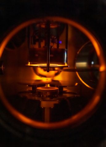
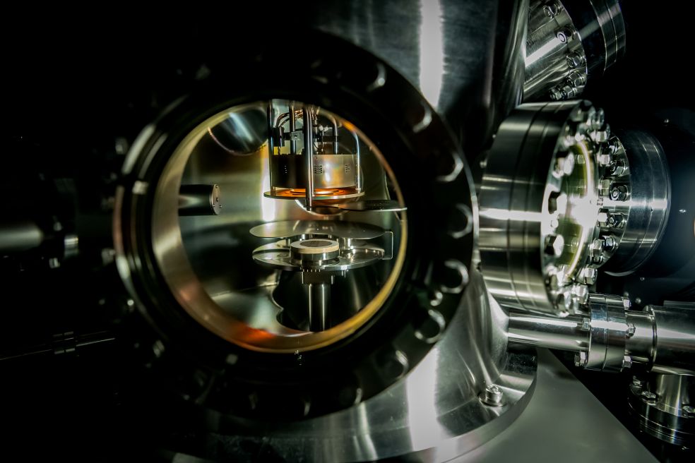
The synthesis takes place by feeding gases into a sealed chamber where they react and form aluminum nitride. The material has several good properties: it is recyclable and a good conductor of heat, which makes it easier to reduce waste heat in the finished components. But the material forms through chemical reactions and physical processes that are not fully understood, and which the researchers need to study in more detail so they can control every step of the process.
Making the impossible possible
In Linköping, a research team led by Igor Abrikosov, a professor of theoretical physics, has developed computational methods that make it possible to predict over 100,000 potential defects in crystalline materials and compile the predictions in a database. The database can then be used to map the defects that can be expected in a given material and plan how the undesirable ones can be avoided while the desirable ones occur. The researchers in Lund will analyze the chemical and physical phenomena as the material takes shape. They plan to recruit another colleague who will help the team to develop an AI tool to streamline the process.
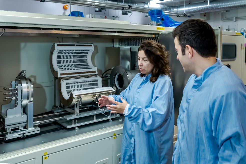
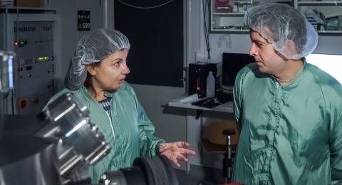
Once the material has been fabricated, it must be carefully analyzed and characterized on atomic level to make sure it works as intended. Researchers led by Per Persson, a professor of materials physics at Linköping University, will study how the atoms are arranged in the material. They will use transmission electron microscopy to make sure the structure is exactly as intended. At Lund University, the team led by visiting professor Mathias Schubert and Vanya Darakchieva will study defects in the material. They will use a new and unique method called terahertz electron paramagnetic resonance to measure the defect charge, electronic structure, and chemical environment. In a final step, a group led by Erik Lind, a professor of nanoelectronics in Lund, will design semiconductor components using the new material.
“He gets the difficult task of proving to the rest of the research community that we really have achieved the impossible. If it works, we will have created a material that performs hundreds or thousands of times better than those currently available.”
The researchers will also be investigating whether the new materials can be used to create quantum networks and quantum sensors that do not require strong cooling to function. But if that succeeds, it is merely a bonus, explains Darakchieva. The main goal is for the project to open a new door for materials researchers – to create materials with precisely the desired properties – something far more significant than merely achieving more efficient semiconductors.
“That is our vision: to allow physicists to cross an entirely new frontier in materials development.”
Text Lisa Kirsebom
Translation Maxwell Arding
Photo Kennet Ruona